 |
 |
 |
| |
|
|
 My MARK 8 |
 ChronWorks.com |
 Apple 1 Software |
About every year I design and build a new clock. This years project is a clock based on an Intel 8008 first generation 8 bit microprocessor. Because it is a fairly unique project Im putting more effort into the documentation. Im also totally opening the design, hardware and software, to anyone wanting to learn more about the 8008. The only requirement I have is this: if you copy or reproduce my information please give me the credit. I spent a good amount of time and effort designing and building the 8008 clock prototype. Ive also tried to do this when Ive used other's information. If you see something on my site where proper credit has not been given, let me know.
Please note that I have done my best to ensure the accuracy of the schematics and PLD algorithms. Each
time I made design changes I did so by updating the schematics first and then the actual prototype. Even
at that there could be errors. I make no guarantees or warranty that building your own 8008 clock will
work. I can only tell you that mine works. If you are fairly experienced and are careful you should be
fine.
I apologize if I wax philosophical too often on this page. Building this clock brought back many memories that occurred over thirty years ago. I was lucky to be a teen in the 70s during the birth of the micro-computer chip. During that period one could not drive down to a store and purchase a home computer as one can today. The computers of that era were university main frames and minis, like the PDP11s, used by Corporations. My first access to a computer began while I was in junior high school. I discovered that I could buy time on the University of Utahs Univac 1108 for one dollar per hour! Unfortunately, non-university students were only allowed to buy a maximum of ten hours per month. So I plunked down my money and with punch card in hand made my way over to a model 43 teletype and thus began one of the most interesting journeys of my life.
At about the same time, articles began to appear in electronic magazines that told of single chip CPU-based computers. I read in fascination about the Intel 8008 microprocessor. As soon as I could get the address on an envelope I sent a letter to Intel asking for a copy the 8008 users manual. I spent hundreds of hours reading and digesting every page of that short document. The Mark 8 edition of Radio Electronics became one of my most treasured possessions. I read and reread every page. I fantasized about being able to afford a board set, and about building a Mark 8. But rather than building a Mark 8, I ended up, designing and building an 8008 computer of my own design, over a three year period. In reality, I probably spent twice what a Mark 8 would have cost. But the educational value of that endeavor was priceless.
Years later, in the late 1990s, I was fortunate enough to exchange email with Jon Titus, the designer of the Mark 8. I had long since lost my original copy of Radio Electronics that contained the Mark 8 plans. Jon was kind enough to mail me a copy of the article and at the time I also discovered that Jon would be traveling to Salt Lake City. While he was in Salt Lake, we met for lunch. Meeting Jon was a truly magical moment. Im not sure if he remembers me, but I will always remember him. Thank you, Jon!
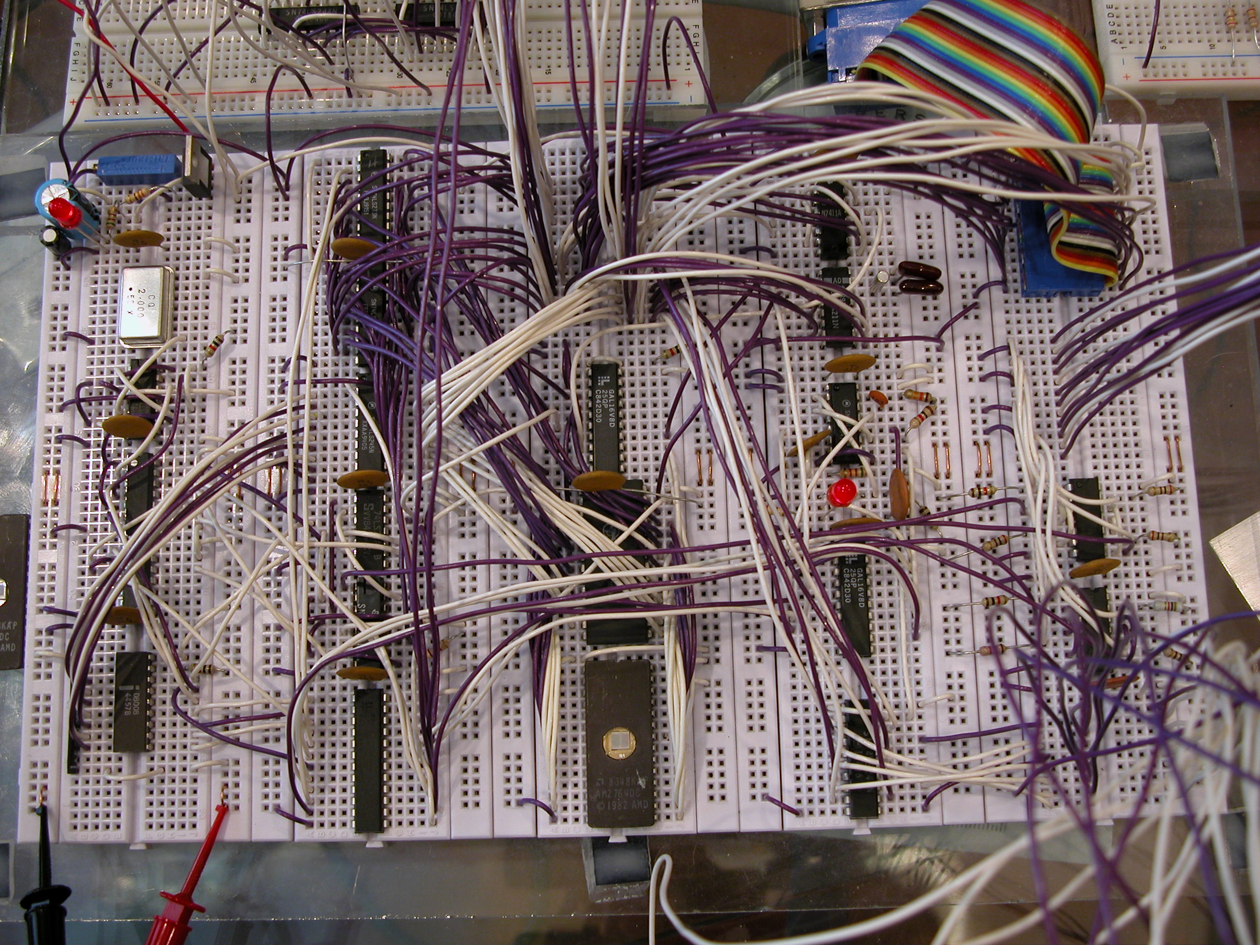
My original 8008 computer utilized nearly one hundred TTL logic chips. The 16k of memory was comprised of one hundred and twenty eight 2102 static rams. I spent hundreds of hours meticulously wire wrapping the processor and IO boards, as well as the back plane. The 16k of 2102 memory chips found their home on four commercial 4k S100 logic boards. For input I used a South West Technical Products ASCII keyboard. For video output I built a text display from a kit sold by Mini Micro Mart. It alone had over 50 ICs. Its design used the same shift register chip set as the Apple I. Even though I had a keyboard and a video display, the real input and output mostly occurred on the front panel using toggle switches and LEDS.
Long before I completed designing and wire wrapping my computer I had hand assembled many lines of code in anticipation of the day when I could actually run the code on my own computer, although in the end, much of that code never was entered. Loading software via the front panel switches was frustratingly laborious! I did however validate that the computer worked. I loaded a monitor that would read keystrokes from the keyboard and display them on a video monitor. That event was the culmination of three years work and proved to be very satisfying.
The motivation to design and build a clock based on the 8008 came from many sources. For several years Ive been designing and building unique clocks. So far, all of them have been built around modern day micro-controller technology while using obsolete display technologies. Using the 8008 offered huge doses of nostalgia. It also turned out to be challenging! Unlike microprocessors today, the 8008 appears almost analog when looking at the slop of the signals emitted by the 8008. To build a computer around an 8008 you have to use a lot of external logic. You also need to compensate for things that just dont work as cleanly as youd expect. Looking back today Im actually quite impressed that my original computer ran. In the 70s I was working on a shoestring budget. My test bench consisted of a cheap low bandwidth single trace oscilloscope and LEDs. I didnt even have the ability to see the delay from clock to sync output, as I do now, not to mention the usefulness of a logic analyzer in understanding the 8008.
The other motivating factor was simply the lack of historical design information published elsewhere or available on the Internet. I want anyone seeking information on how to design or build an 8008 computer to be able to find it more easily than I did. The few sources of information I came upon used very hard to find logic chips (not that you can pick up an 8008 just anywhere). I was disappointed when I found one site where the author would sell a hanging wall piece computer, but only made the information available through NDA. I can understand that approach with something currently in production; but like it or not, there are not enough 8008s in the world, let alone enough interest, to make a living. Also, preserving technology through NDA is akin to Microsofts approach in killing of software products, like DOS, by not publishing the source code. I tend to like preservation through openness, like that of the Linux project. As long as the source is available, the platform becomes moot. Even though my hardware and software probably contain faults, I would rather open my design to public scrutiny, than see useful information about the 8008 die. So here it is
Be aware that I cheated this time around, at least I feel that way. In this design I use many modernly available shortcuts such as programmable logic devices and a high density ram. These devices were not available back in the 70s. In doing so I do not believe I compromised my goal. My goal was to build a clock, not become crippled and blind, wire-wrapping two hundred ICs. Unlike my teenage years, I dont have unlimited time, and I now have a mortgage I no longer mow lawns for a living, as I did at fourteen.
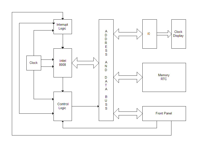
Please understand this is a fully operational 8008 computer. Its 16k of memory space can be configured to use several combinations or RAM and EPROM. I designed in four input and four output ports. It also has a fully functional front panel that can be used to examine or modify memory, or jam in an interrupt instruction. If you are a purest, feel free to convert the PLD algorithms to random logic to build a more authentic computer, though doing so may require modifications to compensate for timing delays. Also remember you cannot load the 8008 down with more than one TTL load. You must buffer all signal lines coming from the CPU. You should also keep in mind that adding more logic chips will increase the power requirements.
The five hundred kilohertz two phase clock required by the 8008 is derived by dividing a two megahertz crystal oscillator by four using two flip flops. Two AND gates then combine the 1 MHZ signal from the first divider stage and the outputs from the final divider stage to produce a two phase non-overlapping clock. Please note that this clock produces a non-compliant signal. Since I AND the signal from the first stage, the system clock produces signals that are shorter than those specified in the Intel spec for the 8008. Each phase is only 500 nanoseconds wide. The Intel 8008 manual specifies a pulse width of 700 nanoseconds for phase one and 550 ns for phase two. If you happen to have an 8008-1 you can substitute a 3.2 Megahertz oscillator to end up with an 800 kilohertz clock. The spec on the 8008-1 calls for a 350 nanosecond pulse on both phases of the clock. Again the clock circuit would produce a shorter pulse of around 313 ns per phase.
For the purest I have included a clock circuit that produces the correct waveform. It uses a 74LS123 dual monostable multivibrator and a few external components. Once the circuit is built you need either an oscilloscope or a logic analyzer to set the pulse widths of the clock. So far Ive noticed no ill affects from the shortened pulse length, although all chips may not be created equal. Ive tried several in my prototype and they have all worked for me. Its your call what you use
Control signals for the 8008 computer are generated using a 22V10 GAL. State lines S0, S1, and S2, the sync line, as well as the high order address bits D6 and D7 are combined to produce bus, memory, and IO control signals. When the computer is in a stopped state the addressed memory location is displayed on the front panel. During the stopped state control signals from the front panel are fed into the 22V10 that allow addressing random memory locations as well as writing to them. The 22V10 also produces signals for interrupt processing. Using the PLD really cuts down the chip count and also the power requirements.
A 74LS245 is used to buffer all data coming to and from the 8008 CPU. When the 8008 is not outputting data the 245 is configured to point data to the CPU. This essentially floats the main data bus. All devices only talk when they are addressed and the respective control signal is enabled. When the processor is in a stopped state the memory read signal (MER) is lowered by default to allow the viewing of memory data on the front panel. Many of the original 8008 designs used multiplexer chips rather than a common data bus. I voted for simplicity by having one common bus.
I use two 74LS273s to latch the address lines. This is done during the T1, T1I, and T2 system cycles. The high address latch contains two bits, D6 and D7, that are routed back and decoded by the 22V10. These bits are used to determine memory read, write and IO cycles.
I opted to use latches, but one could also use four 74LS193s or equivalent. If you plan to load lots of program data by hand using the front panel, using the counter/latches makes the job much easier. You can simply latch in the starting address and then increment or decrement the address counters/latch to the next address and then load the data. This way you only need to set the data switches, deposit the value, increment to the next address, and repeat the process.
The other option would to be to modify the front panel to interface with a printer port. A fairly simple program would let one upload software to the 8008s memory from a PC.
8008 Interrupt Processing Capture
Interrupt logic for my 8008 computer allows you to jam a single instruction into the CPU from the front panel switches. When the interrupt switch is pressed, a signal toggles a 74LS76 flip flop. Next the output of the flip flop routes to a 74LS74 flip flop that is synchronized with the phase one clock of the CPU. This forces the rising edge of the interrupt to be synchronized for correct CPU operation.
Once the CPU recognizes the interrupt request, it outputs a T1I state, which is then latched by another 74LS76 flip flop to create the PINT state. (Process Interrupt). When the PINT state is active the next instruction fetched will come from the front panel. The PINT state is then cleared by the /MER signal. The extra random logic is used to clean up a few glitches inherent in the 8008. Because the 8008 starts up in a stopped state an interrupt is required to get the computer running.
The 8008 is capable of addressing a maximum of 16k bytes of memory. The system includes both RAM and ROM. Using the configuration switches you can select 0k, 2k, 4k, or 8k of ROM, the remainder becomes addressed as RAM. A 16V8 GAL chip provides decoding for the memory as well as the mapping of the RTC if enabled.
I used a 2764, 8k by 8 bit, EPROM for program space. When I am developing programs I use the crash and burn method. That is, write the program, burn it to EPROM, give it a try, and if it crashes I do it all over. Rather that using the 2764 EPROM you could swap it out for a FLASH chip of the same size. Youd still need to program the FLASH chip but youd be ahead with the reduced erasure time.
The RAM chip is a Hitachi HM62256, 32k by 8 bit, static RAM. It actually contains twice as much memory as the 8008 can address, so I only use half. Compared to what I used for memory in my original computer, 2102s that were 1k by 1 bit, the 32k Hitachi chip is amazing. If you again compare this chip to whats available today in modern computers it makes you want to laugh, or cry. The simplicity that a single memory chip adds is fantastic; it would have been unthinkable in the 1970s.
A National Semiconductor NS32FX211 RTC is mapped into the top 16 bytes of memory. This chip is obsolete and difficult to find. I have several that were manufactures samples. The internal oscillator uses a 32.768khz crystal. The main disadvantage of this chip is that there is no provision for battery backup without using external components.
To use a different RTC chip would be reasonably simple. Most of the newer chips I looked at used 32 internal registers, twice as many as the NS32FX211 16 registers. To address more registers does not require a logic change to the 16V8 PLD. To do so you would simply tie the A4 address line to the RTC chip. Then tie the input on pin 13 of the triple input AND gate high, doing so you will map the RTC to the top 32 bytes of memory. You will also have to rewrite the sample code for the clock to utilize the different RTC.
The 8008 I/O is kind of funky by todays standards. Interestingly enough, the output data is sent during the T1 cycle of the CPU to the lower address latch. The address of the port is then latched during the T2 cycle in the high address latch. During the T3 cycle, the 22V10 used the D6/D7 bits to decode the IO operation and further latches the data to the correct IO port latch. If an input port was addressed, the input data is read from one of the input buffers during the T3 cycle. The upper address byte is also used to decode which input port is being read.
I/O port address decoding is done using a 16V8 GAL. The logic is designed to select the first four input and output ports, as designated by the 8008 instructions. If you need a different range, or more I/O ports, you need to make the necessary changes to the 16V8 logic, or add an additional 16V8. The 8008 is capable of addressing a maximum of eight input ports and twenty four output ports.
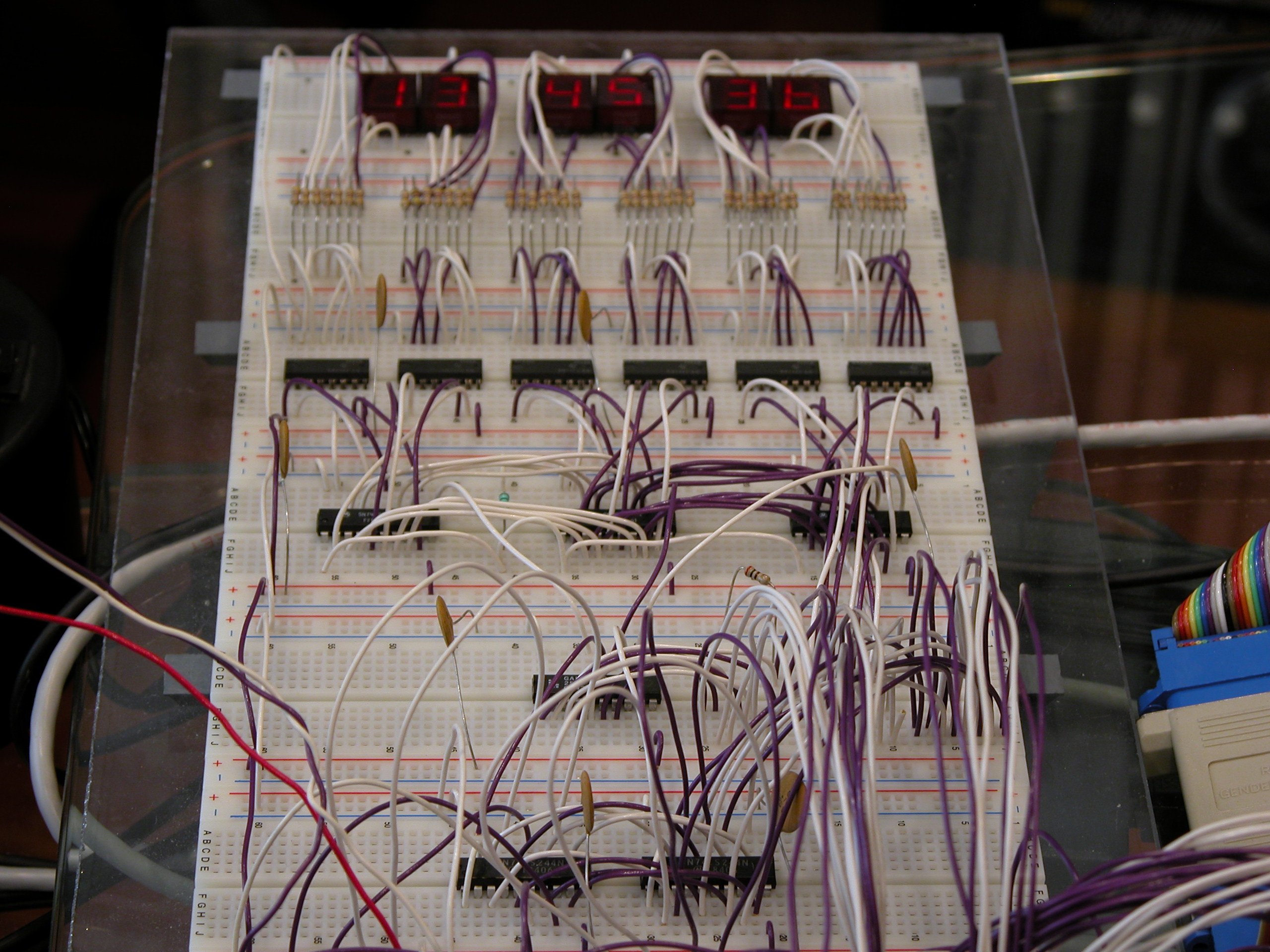
Full traditional front panel functionality exists in my design. LEDs display the address and data bus activity while the computer is running. When the computer is in a stopped state, the contents of the select memory location is displayed. Four momentary switches are used to route the contents of the data switches on the front panel to the low address latch, the high address latch, the selected memory location, or the 8008 data bus during an interrupt request. A 16V8 GAL provides the necessary glue logic to make it all work. In addition, a 74LS123 is used to generate bus and write pulses. There is also an LED that is lit when the computer is running.
In the early days a front panel just seemed so natural. Lots of flashing lights and switches to flip made it so interesting. It was a huge paradigm jump for me when computers started coming without front panels. When designing this computer I knew it had to have a front panel. Even with all of the core control signals in PLDs, putting a front panel on the computer makes it feel right; there must be light.
The display is not necessary if you are not interested in building a stand alone clock. The six 74LS47 LED display drivers are connected using limiting resistors to the seven segment displays. The drivers are connected to output ports 0,1, and 2. The clock software combines the four bit digit codes into one byte for the writes. The display is the simplest part of the entire clock. Ive toyed around with the possibility of using nixie tubes. But in the 70s seven segment LED displays were well in use.
Built and configured as shown here, a suitable power supply needs to provide 5 volts at approximately 1.25 Amps. The 8008 also requires 9 volts at 100 ma when running. To be on the safe side,exceed these values by 50 to 100%. These current draws are based on a computer built using LS TTL chips. Make sure you provide your computer with a well regulated and filtered power supply. I am currently using linear regulators. If you use a switching power supply, verify that the outputs are clean from all switching noise.
Also be aware that you need to use a liberal number of bypass capacitors; TTL is very noisy. Bypass capacitors are not drawn into any of the schematics. I use one .1 uf 25 volt disc capacitor for about every two ICs. Place bypass caps near the VCC connections on the chips, keep the leads short between VCC and ground.
Before powering up your computer verify that all power connections and polarities are correct. Not doing so will ruin your day, especially if you destroy a hard to obtain IC, like the 8008. Measure twice, cut once.
Here is the logic for all of the PLDs. I use WinCUPL, free from Atmel, to compile the logic. And a universal programmer built by Logical Devices to program the GALs.
Nearly all of the parts for the computer can be sourced from Jameco, Digikey, Mouser. The PLDs are Lattice 22V10Ds and 16V8Ds. One word on where to buy the 8008 chips: Ebay. At any given time there are usually several 8008s listed for auction. Ebay hint, dont bid early, doing so only raises the prices. Track the chip until just before the closing of the auction and then bid. Over the years I have collected 8008s whenever I have found them. The purple ceramic and gold chips can be found for about forty to sixty dollars, the all black ceramic chips for about twenty dollars less. So far Ive been lucky; all of my processors work. Be careful when handling the 8008 chips, they are static sensitive. TTL is fairly forgiving, but still use good practices; its a good habit to form.
When running, the processor gets HOT! It runs just over 90 degrees Fahrenheit. All other chips should be relatively cool to the touch, but in reality do generate heat and need ventilation. Keep this in mind if you put your computer in an enclosure.
All resistors are ¼ watt. Bypass caps are disc ceramic .1uf at 25 volts. The caps used on the front panel pulse generation are also disc ceramic. The caps used in the crystal circuit of the RTC should be higher quality, I use silver mica.
Ive scanned one of my original 8008 user manuals. Im also including others Ive found around the internet. My manual published in 1974 lists the newer type instructions.
There are two sets of instructions published for the 8008. The pdf below came from data originating from home.germany.net/nils.eilers/8008/.
The next two files are Excel spreadsheets that contain each instruction and their hexadecimal equivalent.
So far, the software written for the project has been extremely simple. Its main purpose was to verify correct operation of the hardware. The code here simply initializes the RTC and then goes into a loop reading the RTCs data change flag. If a change occurs, the time is read and then written to the output ports connected to the display. To set the time I toggle in the correct values into the RTCs registers mapped in high memory and then interrupt the computer with a restart 0.
The following downloads are for the Scelbi Basic Program from 1974, known as SCELBAL. It was written by Mark Arnold and Nat Wadsworth.
M. G. Arnold and N. Wadsworth, SCELBAL: A Higher Level Language for 8008/8080 Systems, Scelbi Computer Consulting (Milford, CT) 1976.
When I started this project I searched to see if I could locate an assembler for the 8008. I found AS written by Alfred Arnold. I contacted Alfred about an issue on 8008 support. He was kind enough to even add support for the new instruction mnemonics. I run AS in a Linux environment.
Here is the description from his site:
AS is a portable macro cross assembler for a variety of microprocessors and controllers. Though it is mainly targeted at embedded processors and single-board computers, you also find CPU families in the target list that are used in workstations and PCs.
AS works great, thank you Alfred!
During the development of this project I used the following tools.
8008 Interrupt Processing Capture
In my setup I write code and burn it into the 2764 EPROM. It is not necessary to use my methodology in building your own computer. You can either deselect the ROM and enter code directly from the front panel, or build a PC interface to load the memory from a printer port. If you do, please share the information back and Ill post it for others to use.
The 8008 has eight restart vectors. They start at memory location 0 and then every eight bytes from there on. It would be possible to design a more complex interrupt handling system where a device, such as a keyboard, would cause the computer to vector to a specific handler. Since my plans are not that complex Im happy just jamming in a single instruction from the front panel.
One point of interest someone may be able to answer for me. Once Ive started the computer with a
restart instruction I am unable to stop it by jamming in a HLT instruction. Interestingly enough, I do
see the CPU go into a stopped state, and then continue on. To overcome this I simply program a HLT into
the ROM at one of the restart vectors. When I jam in the restart instruction the computer vectors
correctly and stops. Any insight on this would be helpful.
Unlike modern microprocessors the Intel 8008 lacks a hardware stack that can be used to push and pop data in an ad hoc manner. Tom Pittman designed a solution for the 8008 that uses 6 TTL chips to create a 16 byte stack.
| Copyright © 2004-2021, Len Bayles | Thu Sep 9 02:53:44 UTC 2021 |